UD’s Anderson Janotti predicts surface structure of advanced electronic materials
The next great technological innovation, the color television or iPhone of our time, might be enabled by novel advanced electronic materials called Heuslers.
What are Heusler materials? Named for the German mining engineer and chemist Friedrich Heusler, they are complex intermetallics, solid compounds with one or more metallic elements. Many exhibit tunable, or adjustable, electronic properties. Examples include magnetism, superconductivity and topological band structure—all of which are important to scientists developing electronic devices.
However, just as toast needs to be slathered with butter or jam to be breakfast-worthy, Heusler materials must be combined with other materials for use in devices. The performance of Heusler materials in devices will crucially depend on their surface or interface with other materials—just as the melted butter on the surface of toast transforms it from dry to delicious.
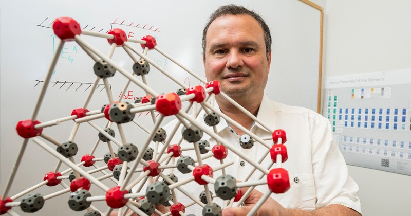
Therefore, to harness the power of these materials, physicists, materials scientists and engineers must first understand their surfaces and interfaces, down to atom by atom. Anderson Janotti, an assistant professor in materials science and engineering at the University of Delaware, is at the forefront of this field. He models the surfaces of electronic materials, the places where electrons meet and interact, imbuing the materials with special properties. Slight rearrangements of the atoms at the surface can lead to drastic changes of properties.
Janotti and Abhishek Sharan, a graduate student in physics at UD, worked with a team of experimentalists to model the surfaces of half-Heusler compounds, particularly promising electronic materials. Their “electron counting model” explains the atomic and electronic structure at these surfaces and could help other scientists and engineers utilize these materials more effectively going forward. It is described in a paper recently published in Science Advances.
We asked Janotti to explain the promise of the advanced electronic materials—and this leap forward in understanding about them.
Question: Why are scientists so excited about Heusler materials?
Answer: This is an emerging class of materials that could be used in many device applications, including thermoelectrics, converting heat into electricity for energy savings and more. The most promising is in spintronics for efficiency of data storage and transfer, and quantum computing, which could be utilized to perform calculations beyond what even today’s supercomputers can handle. We expect that our findings will help in the development of these materials for energy-related applications, from thermoelectrics to quantum computers and more.
Q: Why do you study the surfaces of Heusler materials?
A: For any device for electronics, you really need to know what happens at the surface. Controlling the surface is key to improving the device performance. The surfaces of these materials have broken bonds that can trap electrons or release electrons, usually scattering electrons from inside the material. When two materials come together, there are properties that emerge just because of the surface or interface and the behavior of these electrons. Nobel Laureate Herbert Kroemer said the properties of the surface are what make the device.
Q: How do you investigate these materials?
A: Our collaborators at UC-Santa Barbara, led by Chris Palmstrøm and Jason Kawasaki, now at the University of Wisconsin, grow the material using molecular beam epitaxy, depositing the elements atomic layer by atomic layer. We do the theory part. It takes a combination of theory and experiments to understand the surface of these complex materials. It’s back and forth. Sometimes they come to us with experimental results for us to explain. Sometimes we can predict properties that they can go into the lab and try to measure.
Q: How does the electron counting model work? How do you count the electrons, exactly?
A: All materials are made of atoms, with the nuclei at the center surrounded by a cloud of electrons. Atoms form bonds by sharing some of their electrons with one another. Crystals consist of a large number of atoms bonded together in a regularly arranged and repetitive pattern. This pattern is broken at crystal surfaces or interfaces, leaving some atoms without partners and unshared electrons in dangling bonds. Rearrangements of the atoms at the surface or interface, driven to heal the broken bonds, and the resulting electronic properties usually overshadow the properties of the bulk material in devices. Understanding why and how these rearrangements occur is, therefore, a key problem.
In many simple cases of insulator or semiconductor materials, the possible structures of the surface are governed by basic chemistry rules, such as having two electrons per bond. One just sums all the electrons each atom brings to the surface and compares with the number of electrons in possible bonds formed at the surface. If all the electrons are accounted for, the structure is likely to be stable.
Scientists assumed that the electron clouds for the metallic elements that make up half-Heusler materials were too complicated for such basic counting rule. It was surprising to us that the predicted stable surfaces in our simulations of these complex materials, composed solely metallic elements, could be explained by such simple rules.
Combining computer simulations and experiments we predicted and confirmed the surface configuration for an important half-Heusler material called cobalt titanium antimony, which is a potentially useful semiconductor. The stable surface structures of this complex material were then explained by a simple electron counting rule. The same simple method was then applied to other two half-Heusler compounds, a semimetal and a ferromagnet, and the plan is to identify more promising materials.
Q: How do you do your calculations?
A: The equations are known. The theory behind it is quantum mechanics. We can model a surface, but then we have so many electrons that we cannot solve it analytically. We have to solve it numerically with approximations that have been developed over the years. Nowadays we have supercomputers that can actually handle such problems. We tap into a supercomputing facility in Pittsburgh and use 200 to 400 computer cores at once. Each calculation can take a day or two, and we have to do many of those calculations. We use density functional theory, a state-of-the-art electronic structure method where you determine the behavior of electrons, chemical bonds at the materials surface or the interface of the two materials. We call these first-principles calculations because we don’t use any parameters from experiments. We know what elements we have, in this case, cobalt, titanium and antimony, and more or less their positions in the crystal, and that’s it. That’s all we assume.
Q: How did your calculations contribute to the development of the model?
A: Experimentally, the team in California grows the material, looks at images through a scanning tunneling microscope and obtains chemical composition through element-specific x-ray photoemission measurements. Then, they can change some of the parameters, like the supply of a given element during growth. Then, they need an interpretation for what they see. The interpretation comes when we actually solve the quantum mechanical problem of electrons moving in the field of the nuclei for all possible surface structures. It basically can tell the electronic charge distribution for a given configuration’s atomic positions. We can directly simulate a microscopic image that they can actually measure, so the calculations correspond to the experimental data. The stable surface structures are determined by their total energies, which include electronic, strain, bond breaking and formation effects.
We can see, for example, that when certain atoms are missing, others approach each other and form bonds. We can tell them the exact position of the atoms based on the simulation. And we can tell them which surface structure are stable in which conditions. We can predict what they will see when they change the concentrations of the different elements.
Q: Where will this work go next?
A: The implications are quite general. The electron counting model that we developed is basically a model to explain the reconstruction in this wide class of materials that all have the same Heusler crystal structure. These materials can be topological, half-metals or superconductors, and now we actually have a model to understand how the surface will influence other measurements.
The research was supported by the U.S. Department of Energy (DE-SC0014388), the National Science Foundation Extreme Science and Engineering Discovery Environment (ACI-1053575), the Wisconsin Alumni Research Foundation and the UW-Madison Materials Research Science and Engineering Center (AQ41 NSF DMR-1121288).


